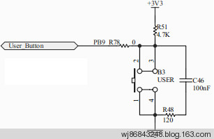
User Button硬件連接如下圖所示:當(dāng)按鍵被按下,PB9檢測到低電平,相反PB9被3.3V電源拉高。 
LED硬件連接如下圖所示:高電平點亮LED。

要想將PB9管腳配置成輸入模式,程序所需如下步驟:(必須的) 第一步:配置系統(tǒng)時鐘。見STM32F103x RCC寄存器配置 除此之外,還需將GPIO外設(shè)時鐘打開。 /* Enable GPIOC and GPIOB clock */
RCC_APB2PeriphClockCmd(RCC_APB2Periph_GPIOB, ENABLE);
RCC_APB2PeriphClockCmd(RCC_APB2Periph_GPIOC, ENABLE);
第二步:配置中斷向量表。決定將程序下載到RAM中還是FLASH中。以后講。void NVIC_Configuration(void)
{
#ifdef VECT_TAB_RAM
/* Set the Vector Table base location at 0x20000000 */
NVIC_SetVectorTable(NVIC_VectTab_RAM, 0x0);
#else /* VECT_TAB_FLASH */
/* Set the Vector Table base location at 0x08000000 */
NVIC_SetVectorTable(NVIC_VectTab_FLASH, 0x0);
#endif
}
第三步:配置GPIO的模式。輸入模式還是輸出模式。STM32_GPIO配置及庫函數(shù)講解——LED跑馬燈已講過。 void GPIO_Configuration(void)
{
GPIO_InitTypeDef GPIO_InitStructure;
/* Configure PC.06, PC.07, PC.08 and PC.09 as Output push-pull */
GPIO_InitStructure.GPIO_Pin = GPIO_Pin_6 | GPIO_Pin_7 | GPIO_Pin_8 | GPIO_Pin_9;
GPIO_InitStructure.GPIO_Speed = GPIO_Speed_50MHz;
GPIO_InitStructure.GPIO_Mode = GPIO_Mode_Out_PP;
GPIO_Init(GPIOC, &GPIO_InitStructure);
/* Configure PB.09 as Input pull-up */
GPIO_InitStructure.GPIO_Pin = GPIO_Pin_9;
GPIO_InitStructure.GPIO_Mode = GPIO_Mode_IPU; //上拉輸入
GPIO_Init(GPIOB, &GPIO_InitStructure);
} 第四步:讀該管腳上的電平狀態(tài)。需要介紹一個庫函數(shù)。
v GPIO_ReadInputDataBit 從指定Port指定Pin,讀該管腳上的電平狀態(tài):
u8 GPIO_ReadInputDataBit(GPIO_TypeDef* GPIOx, u16 GPIO_Pin)
{
u8 bitstatus = 0x00;
/* Check the parameters */
assert_param(IS_GPIO_ALL_PERIPH(GPIOx));
assert_param(IS_GET_GPIO_PIN(GPIO_Pin));
if ((GPIOx->IDR & GPIO_Pin) != (u32)Bit_RESET)
{
bitstatus = (u8)Bit_SET;
}
else
{
bitstatus = (u8)Bit_RESET;
}
return bitstatus;
} 涉及到GPIO_IDR寄存器,如下所示 

經(jīng)過上面4步,就可以檢測PB9管腳的電平狀態(tài)。
按鍵按下,PB9管腳應(yīng)該是低電平,怎么才能驗證,最簡單的方法是:當(dāng)按鍵被按下,點亮所有LED。
下面給出完整程序: /* Includes ------------------------------------------------------------------*/
#include "stm32f10x_lib.h"
/* Private function prototypes -----------------------------------------------*/
void RCC_Configuration(void);
void NVIC_Configuration(void);
void GPIO_Configuration(void);
void Delay(vu32 nCount);
/*******************************************************************************
* Function Name : main
* Description : Main program.
* Input : None
* Return : None
*******************************************************************************/
int main(void)
{
#ifdef DEBUG
debug();
#endif
/* Configure the system clocks */
RCC_Configuration();
/* NVIC Configuration */
NVIC_Configuration();
/* Configure the GPIO ports */
GPIO_Configuration();
/* Infinite loop */
while (1)
{
if (GPIO_ReadInputDataBit(GPIOB, GPIO_Pin_9) == 0) //檢測USR鍵是否被按下,若按下,則點亮全部LED
{
GPIO_SetBits(GPIOC, GPIO_Pin_6 | GPIO_Pin_7 | GPIO_Pin_8 | GPIO_Pin_9);
}
else
{
GPIO_ResetBits(GPIOC, GPIO_Pin_6 | GPIO_Pin_7 | GPIO_Pin_8 | GPIO_Pin_9);
}
}
}
/*******************************************************************************
* Function Name : RCC_Configuration
* Description : Configures the different system clocks.
* Input : None
* Return : None
*******************************************************************************/
void RCC_Configuration(void)
{
ErrorStatus HSEStartUpStatus;
/* RCC system reset(for debug purpose) */
RCC_DeInit();
/* Enable HSE */
RCC_HSEConfig(RCC_HSE_ON);
/* Wait till HSE is ready */
HSEStartUpStatus = RCC_WaitForHSEStartUp();
if (HSEStartUpStatus == SUCCESS)
{
/* Enable Prefetch Buffer */
FLASH_PrefetchBufferCmd(FLASH_PrefetchBuffer_Enable);
/* Flash 2 wait state */
FLASH_SetLatency(FLASH_Latency_2);
/* HCLK = SYSCLK */
RCC_HCLKConfig(RCC_SYSCLK_Div1);
/* PCLK2 = HCLK */
RCC_PCLK2Config(RCC_HCLK_Div1);
/* PCLK1 = HCLK/2 */
RCC_PCLK1Config(RCC_HCLK_Div2);
/* PLLCLK = 8MHz * 9 = 72 MHz */
RCC_PLLConfig(RCC_PLLSource_HSE_Div1, RCC_PLLMul_9);
/* Enable PLL */
RCC_PLLCmd(ENABLE);
/* Wait till PLL is ready */
while(RCC_GetFlagStatus(RCC_FLAG_PLLRDY) == RESET) {}
/* Select PLL as system clock source */
RCC_SYSCLKConfig(RCC_SYSCLKSource_PLLCLK);
/* Wait till PLL is used as system clock source */
while(RCC_GetSYSCLKSource() != 0x08) {}
}
/* Enable GPIOC and GPIOB clock */
RCC_APB2PeriphClockCmd(RCC_APB2Periph_GPIOB, ENABLE);
RCC_APB2PeriphClockCmd(RCC_APB2Periph_GPIOC, ENABLE);
}
/*******************************************************************************
* Function Name : NVIC_Configuration
* Description : Configures Vector Table base location.
* Input : None
* Return : None
*******************************************************************************/
void NVIC_Configuration(void)
{
#ifdef VECT_TAB_RAM
/* Set the Vector Table base location at 0x20000000 */
NVIC_SetVectorTable(NVIC_VectTab_RAM, 0x0);
#else /* VECT_TAB_FLASH */
/* Set the Vector Table base location at 0x08000000 */
NVIC_SetVectorTable(NVIC_VectTab_FLASH, 0x0);
#endif
}
/*******************************************************************************
* Function Name : GPIO_Configuration
* Description : Configures the different GPIO ports.
* Input : None
* Return : None
*******************************************************************************/
void GPIO_Configuration(void)
{
GPIO_InitTypeDef GPIO_InitStructure;
/* Configure PC.06, PC.07, PC.08 and PC.09 as Output push-pull */
GPIO_InitStructure.GPIO_Pin = GPIO_Pin_6 | GPIO_Pin_7 | GPIO_Pin_8 | GPIO_Pin_9;
GPIO_InitStructure.GPIO_Speed = GPIO_Speed_50MHz;
GPIO_InitStructure.GPIO_Mode = GPIO_Mode_Out_PP;
GPIO_Init(GPIOC, &GPIO_InitStructure);
/* Configure PB.09 as Input pull-up */
GPIO_InitStructure.GPIO_Pin = GPIO_Pin_9;
GPIO_InitStructure.GPIO_Mode = GPIO_Mode_IPU; //上拉輸入
GPIO_Init(GPIOB, &GPIO_InitStructure);
}
/*******************************************************************************
* Function Name : Delay
* Description : Inserts a delay time.
* Input : nCount: specifies the delay time length.
* Return : None
*******************************************************************************/
void Delay(vu32 nCount)
{
for(; nCount != 0; nCount--);
}
#ifdef DEBUG
/*******************************************************************************
* Function Name : assert_failed
* Description : Reports the name of the source file and the source line number
* where the assert_param error has occurred.
* Input : - file: pointer to the source file name
* - line: assert_param error line source number
* Return : None
*******************************************************************************/
void assert_failed(u8* file, u32 line)
{
/* User can add his own implementation to report the file name and line number,
ex: printf("Wrong parameters value: file %s on line %d\r\n", file, line) */
/* Infinite loop */
while (1)
{
}
}
#endif
還有個問題:PB9的初始狀態(tài)是什么?或者說GPIO_Configuration函數(shù)后PB9管腳上是高電平還是低電平? 這要看GPIO_InitStructure結(jié)構(gòu)體的GPIO_Mode成員變量初始化為什么,如果為上拉,則PB9管腳為高電平;如果為下拉,則PB9管腳為低電平。
GPIO管腳內(nèi)部電路設(shè)計如圖: 
當(dāng)GPIO初始化為輸入上拉模式,由上圖可知:該端口向外輸出高電平,即:ODR對應(yīng)位為1 當(dāng)GPIO初始化為輸入下拉模式,由上圖可知:該端口向外輸出低電平,即:ODR對應(yīng)位為0
如何調(diào)試:在下面兩處處設(shè)個斷點。 1. GPIO初始化函數(shù)GPIO_Configuration中 
可以看到:當(dāng)GPIO設(shè)置成輸入上拉模式時,等待GPIO初始化完畢,該管腳ODR9為1
2. 在main函數(shù)中,設(shè)置一個斷點。 
全速執(zhí)行(F5),按住User Button不放,可以看到GPIOB_IDR的IDR9=0。當(dāng)放開按鍵時,再單步調(diào)試(F10), GPIOB_IDR的IDR9=1。
總結(jié):1. GPIO配置成輸入模式時,最好配置成浮空輸入(ODR對應(yīng)位為0)。上拉、下拉只是該管腳初始化完對外表現(xiàn)的電平狀態(tài)。
2. GPIO配置成輸入模式,只關(guān)心GPIO_IDR寄存器。檢測該管腳外部輸入的是高電平還是低電平。
3. GPIO配置成輸出模式,只關(guān)心GPIO_ODR寄存器。通過該管腳向外部輸出高電平還是低電平。
|