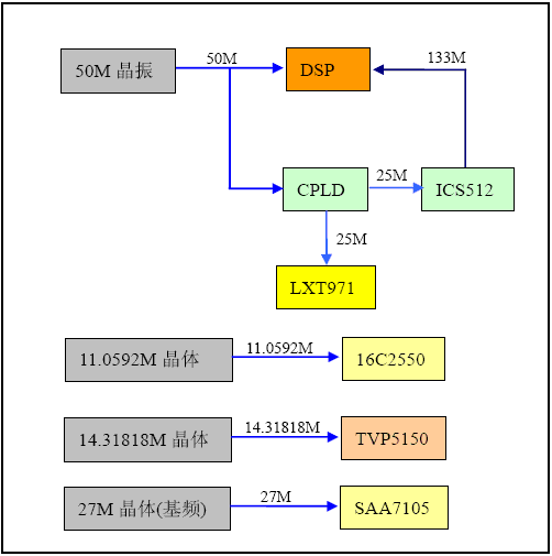
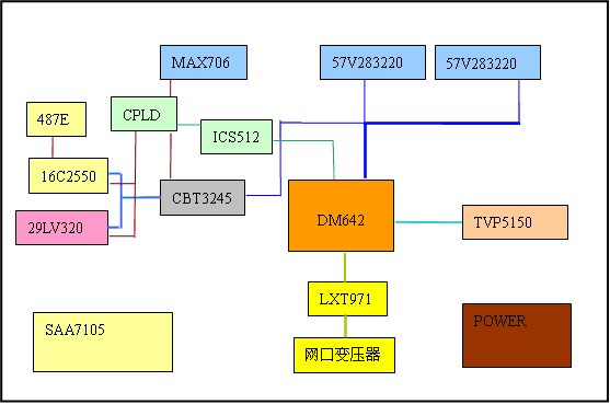
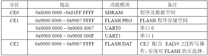
JD642電源設計:
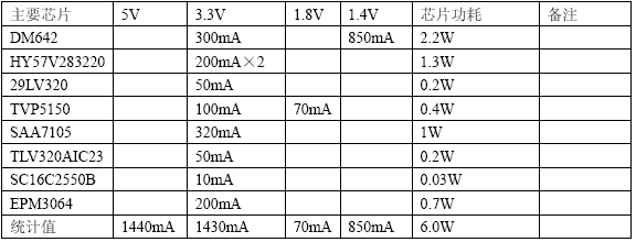
各電源均由5V電源轉換得到(所需電流值為(1430*3.3/90%+70*5+850*1.4/85%)/5=1440mA)。1.4V和3.3V均使用MAX1951ESA提供,1MHz的開關頻率能極大的降低濾波需求,雖然芯片成本高一些,但提高了系統的電源利用率,降低了對5V供電的需求,很大程序上提高了模塊的可移植性。另外,電源濾波全部使用瓷片電容,不但提高了性能,還能對電源芯片提高的成本有很大補償。1.8V由LM1117-18得到。
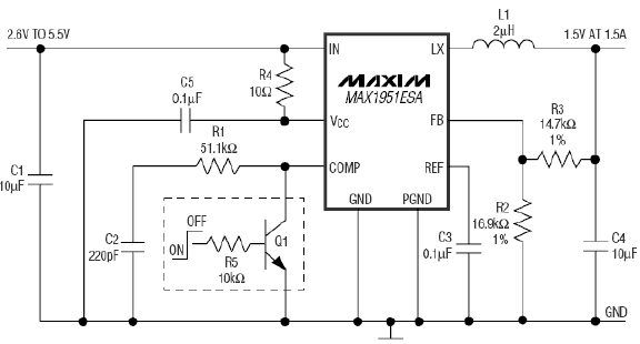
FB腳電壓達到0.8V時回路穩定,輸出電壓VO=0.8V*(1+R3/R2)。
R1和C2是用于補償L1和輸出濾波電容諧振效果,保證在整個頻帶內能提供穩定的電源,需根據輸出電流大小和L1、C4值進行計算,計算方法見MAX1951數據手冊。
下面是DM642數據手冊里對DSP電源電容分布的要求:
In order to properly decouple the supply planes from system noise, place as many capacitors (caps) as possible close to the DSP. Assuming 0603 caps, the user should be able to fit a total of 60 caps, 30 for the core supply and 30 for the I/O supply. These caps need to be close to the DSP power pins, no more than 1.25 cm maximum distance to be effective. Physically smaller caps, such as 0402, are better because of their lower parasitic inductance. Proper capacitance values are also important. Small bypass caps (near 560 pF) should be closest to the power pins. Medium bypass caps (220 nF or as large as can be obtained in a small package) should be next closest. TI recommends no less than 8 small and 8 medium caps per supply (32 total) be placed immediately next to the BGA vias, using the "interior" BGA space and at least the corners of the "exterior".
Eight larger caps (4 for each supply) can be placed further away for bulk decoupling. Large bulk caps (on the order of 100 μF) should be furthest away (but still as close as possible). No less than 4 large caps per supply (8 total) should be placed outside of the BGA.
綜上:DSP芯片附近電源電容需求如下:
0402封裝1nF電容16*2個
0603封裝0.1uF電容8*2個
10uF瓷片電容2*2個
220uF鉭電容2*2個
上面組合應可滿足DSP芯片電源對C、ESR、ESL需求。因采用高頻開關電源,鉭電容應當可以不焊,視調試情況決定是否保留。(后經樣板調試驗證可以去掉全部鉭電容)
|


 QQ好友和群
 QQ空間
QQ空間 騰訊微博
騰訊微博 騰訊朋友
騰訊朋友 收藏
收藏 淘帖
淘帖 頂
頂 踩
踩